Welcome to sysilicon.com


Research and development
R&D history
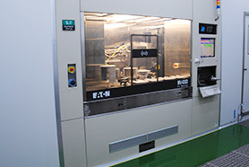
The company has R&D bases in the United States and Taiwan, making full use of the human, intellectual and equipment resources of the Central University and Taiwan Industrial Research Institute for technological innovation and intellectual property development, as well as the information and perfect IC industry foundation of Silicon Valley in the United States before official production. Production process development demonstration; at the end of 2008, the 8-inch SOI production process was completely applied to the company's production line, conducting new technology feasibility test and development, and the technology process and industrialization process were demonstrated and improved. It has laid a good foundation for industrialization in Shenyang. At the end of 2014, the company has completed mass production of SOI and epitaxial wafers.

R&D background
The company's main technology source is the Chinese overseas study doctor, familiar with and master SOI, sSOI wafer manufacturing process and technology. With its unique SOI wafer manufacturing technology, it has established an SOI wafer production line in Shenyang to provide high-quality SOI wafers.

Intellectual property
TM-SOI technology is a proprietary SOI wafer manufacturing method that enables the third generation of “silicon wafer bonding and film transfer” thin film SOI wafer processing.
The company has TM-SOI independent intellectual property rights and a full set of SOI wafer processing technology.
Address: No. 15-22, hunnan Road, Shenyang Export Processing Zone, Liaoning